
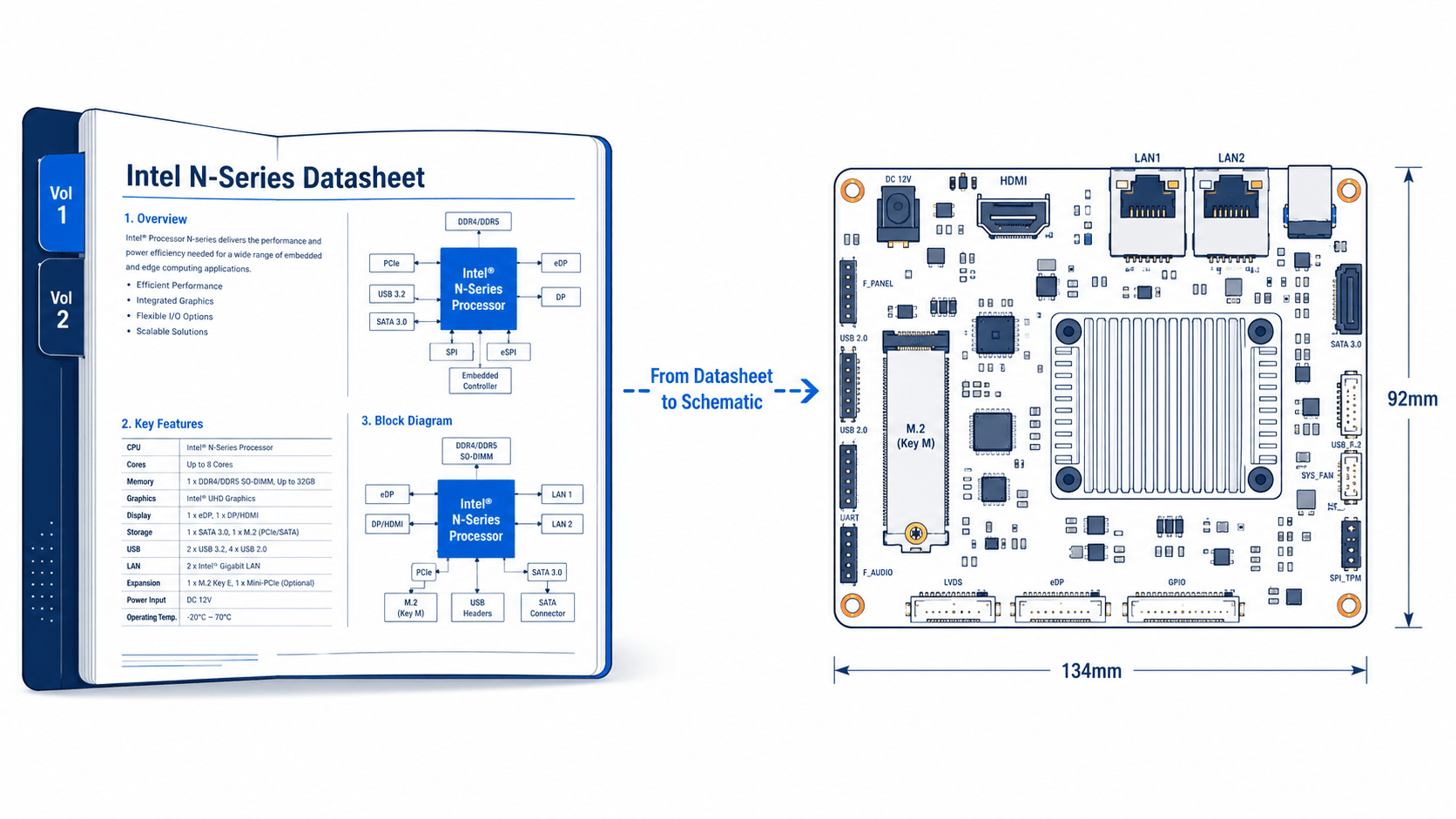
The Intel N100 datasheet (Volumes 1 and 2) is the foundation of every custom carrier board built around Intel's 12th Gen Alder Lake-N processor. This guide walks through the chapters that matter, deconstructs a publicly available reference schematic, and shows how to translate spec-sheet numbers into a working power tree—using the youyeetoo K1 carrier (134×92mm) as a worked example.
This is the hardware-engineering companion to our Embedded Integration Guide, which covers module selection. Read that first if you are still choosing between SOM, complete SBC, and Mini PC. This article assumes you have chosen "design my own carrier" and need to know what to read, what to draw, and what not to miss.
| Parameter | Value | Datasheet Reference |
|---|---|---|
| TDP | 6W (configurable 4.5W–25W) | Vol 1 — Thermal Management Support |
| Cores / Threads | 4 / 4 | Intel ARK |
| Base / Turbo Clock | 0.8 GHz / 3.4 GHz | Intel ARK |
| L3 Cache | 6 MB | Intel ARK |
| Memory Support | LPDDR5 / DDR4 / DDR5, up to 16 GB | Intel ARK |
| PCIe Lanes | 9 lanes (3.0) | Vol 1 — Supported Technologies |
| Display Pipes | 3 (any combination of HDMI / DP / eDP / MIPI) | Vol 1 — Supported Technologies |
| Operating Temp | 0°C to 105°C (Tjmax) | Vol 1 — Thermal Management Support |
All values verified against Intel ARK and the Intel N-Series Datasheet on 2026-05-25.
The Intel N100 datasheet is the official electrical, thermal, and mechanical specification for the N-Series, published by Intel as two public PDFs: Vol 1 (Datasheet, Volume 1 of 2) and Vol 2 (Datasheet, Volume 2 of 2). Together they total several hundred pages.
Most engineers do not need to read the entire document. Vol 1 is organized around eight functional chapters; the ones that ship products are:
Vol 2 covers signal-integrity guidelines and routing rules: trace impedance targets, length-matching tolerances, and via-stitching patterns for high-speed signals.
Practical reading order: Thermal → Power → Supported Technologies (memory + PCIe) → Ball-out → Vol 2 (signal integrity). Save display-pipe details for the subsystem-design phase.
The datasheet is freely downloadable under content IDs 788130 (Vol 1) and 788131 (Vol 2). Treat it as authoritative whenever a third-party reference contradicts it.
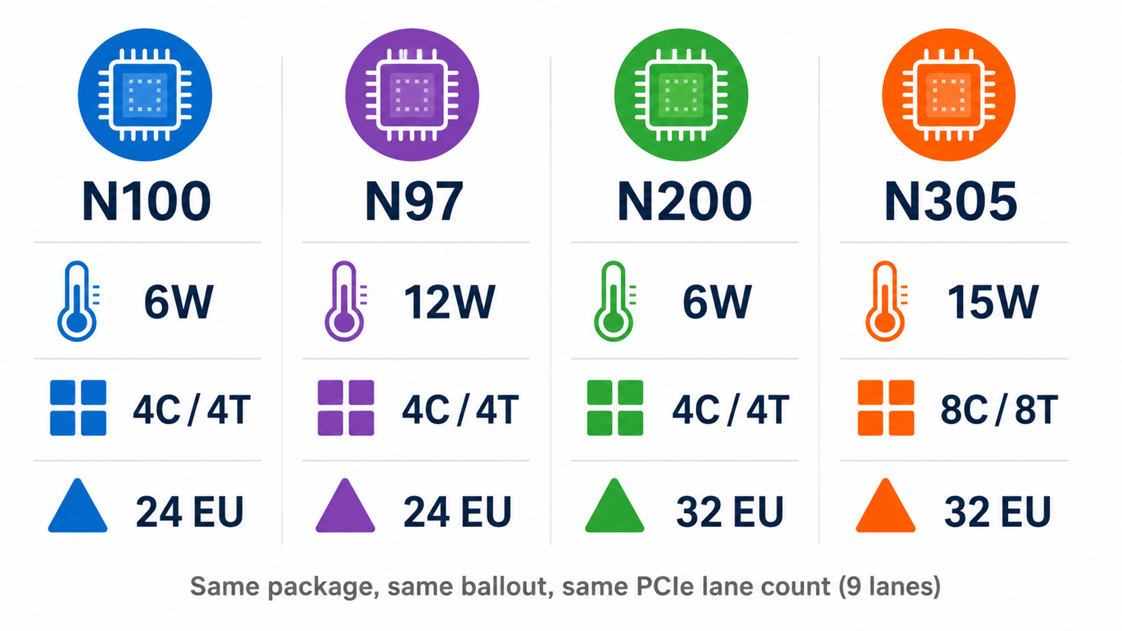
If you are choosing between N-Series SKUs, the choice is mostly TDP, core count, and PCIe lanes—not raw clock speed. All four parts share the same Alder Lake-N silicon and similar I/O.
| SKU | TDP | Cores / Threads | Turbo | GPU EUs | PCIe Lanes |
|---|---|---|---|---|---|
| N100 | 6W (4.5–25W cTDP) | 4 / 4 | 3.4 GHz | 24 | 9 |
| N97 | 12W | 4 / 4 | 3.6 GHz | 24 | 9 |
| N200 | 6W (4.5–15W cTDP) | 4 / 4 | 3.7 GHz | 32 | 9 |
| N305 | 15W | 8 / 8 | 3.8 GHz | 32 | 9 |
Selection logic:
The carrier-board design is essentially identical across all four. Choose the SKU; design once.
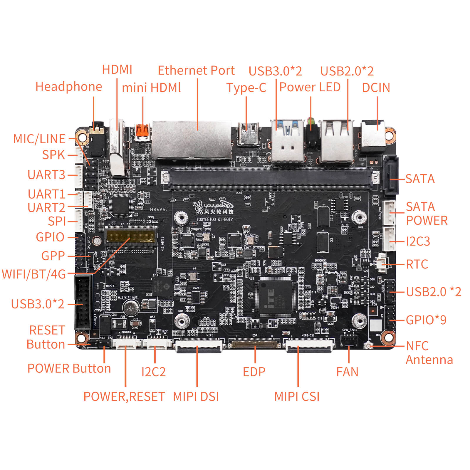
Most N100 reference schematics live behind NDAs. The youyeetoo K1 carrier-board schematic is one of the few publicly downloadable—via the Schematic Diagram section of the K1 wiki, which provides current download links (official drive plus a Google Drive mirror). Treat it as a worked example, not a copy-paste template.
The K1 carrier (134×92mm) breaks into five functional blocks:
Reading tip: open the schematic alongside the Vol 1 ball-out chapter. Every signal leaving the SOM connector should map to a ball in the Ball-out Information chapter; every power rail should map to a rail named in the Power Management Support chapter. If something does not match, you have either misread the schematic or the SOM is doing something custom.
What is not public: SOM-internal layout, the LDO chain on the SOM, and BIOS-controlled signal routing. You design against the carrier-side of the connector, not the chip-side.
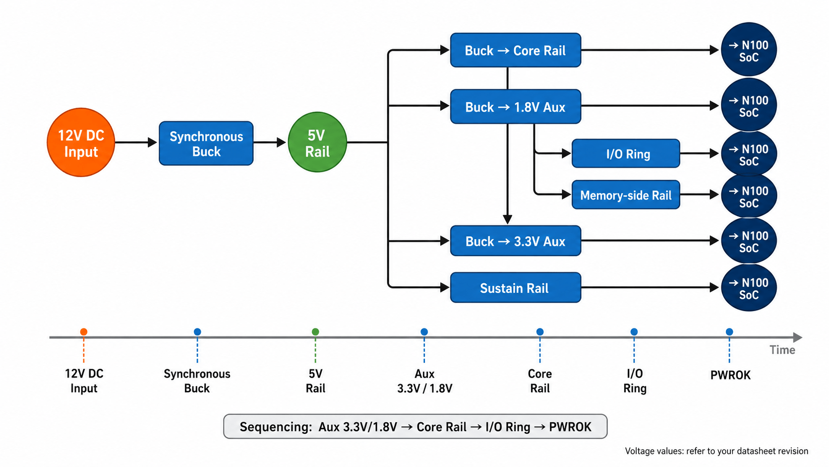
The power tree is the directed graph of voltage conversion stages from the wall-plug input down to every silicon pin. For an N100 design it must satisfy two constraints: deliver the right voltage at the right current, and deliver them in the right order.
How to read your N100 power rail set (Vol 1 — Power Management Support):
The N100 datasheet defines a set of named power rails — typically including a primary input rail (VCCIN_AUX), a core rail under FIVR/DLVR control, an I/O rail (VCCIO), a memory-side rail (VDDQ for the memory interface, VCCSA for the system agent), plus 1.8V and 3.3V auxiliary rails. Voltage levels and exact rail names vary by datasheet revision and silicon stepping — always copy them from your binding datasheet, not from a third-party guide. What is universal across revisions is the topology: a 12V or 5V external source supplies an input rail, which then derives several internal/external rails through bucks and LDOs.
Sequencing requirements (Vol 1 — Power Management Support): the auxiliary 3.3V and 1.8V rails must come up before the main core/input rail; the core and sustain rails must rise within a tight window of each other; the I/O ring must reach steady state before any reference clock is enabled; PWROK is the last signal asserted. Violating any of these typically results in "the board powers on but never boots"—the most expensive bug to diagnose because it has no error message.
A 7-step power-tree workflow:
Common pitfalls (each tied to a datasheet chapter):
K1 measured power at 12V input: idle 4.2 W, typical 6–8 W, peak 12 W. A 12V/2A supply (24 W) provides comfortable margin.
The Intel N100 supports three independent display pipes (Vol 1 — Supported Technologies). All four interface families—HDMI, DisplayPort, eDP, and MIPI DSI—share these three pipes through programmable muxing. The carrier board decides which physical port each pipe routes to.
On the K1 carrier, this mux is exposed at BIOS level: MIPI DSI, eDP, and Type-C DisplayPort are a 3-choose-1 group. Switching requires a BIOS firmware reflash. HDMI and Mini HDMI are always available and use the remaining pipes.
Practical multi-display configurations:
Each active display pipe adds 0.5–1.2 W to VCCIN load. Triple-display configurations should be sized at the upper end of the 4 A VCCIN budget.
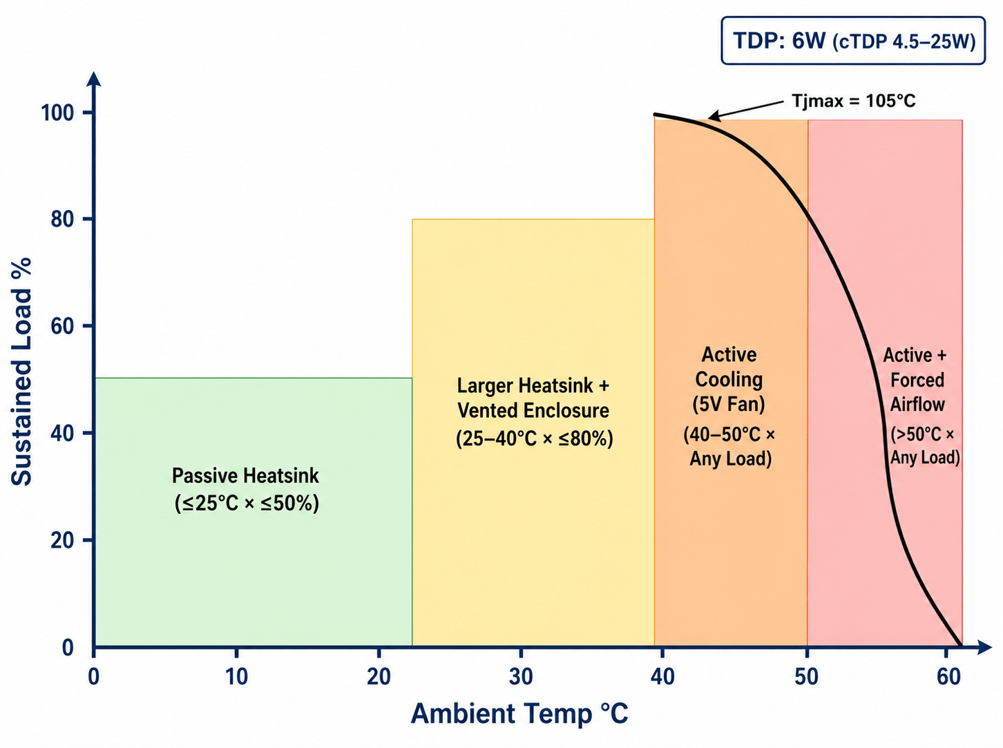
The N100 datasheet specifies Tjmax = 105°C and a TDP of 6W with cTDP-down to 4.5 W and cTDP-up to 25 W (Vol 1 — Thermal Management Support). Whether you can run fanless depends on three numbers: ambient temperature, enclosure thermal resistance, and sustained load.
| Ambient | Sustained Load | Cooling Approach |
|---|---|---|
| ≤ 25°C | Intermittent (≤50% CPU) | Aluminum heatsink, no fan |
| 25–40°C | Continuous (≤80% CPU) | Larger heatsink, vented enclosure |
| > 40°C | Continuous | Active cooling (5V fan) or forced airflow |
| > 50°C | Any | Active cooling + ventilation, no exceptions |
Wide-temperature deployments (-20°C to 60°C, K1's published range) require attention beyond the datasheet: LPDDR5 timing margins shrink below 0°C—validate boot at -20°C. Use X7R or X8R MLCCs on power rails; standard X5R drops capacitance sharply below -10°C, causing rail droop on cold boot. In dusty 24/7 enclosures, conformal coating helps but must not migrate onto SOM connector contacts.
K1 is rated -20°C to 60°C with passive heatsink under typical load. Sustained 100% CPU at 60°C ambient is the boundary case; production deployments at that boundary should add a fan.
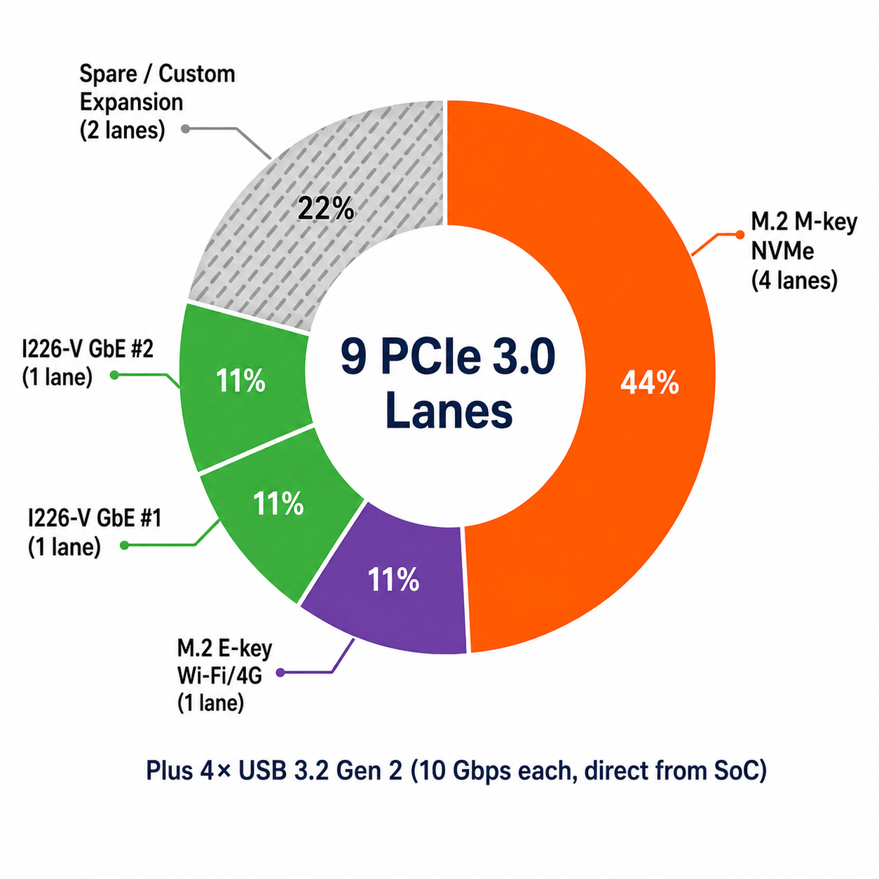
The N100 exposes nine PCIe 3.0 lanes plus two USB 3.2 Gen 2 host controllers (Vol 1 — Supported Technologies). On the K1 carrier these are allocated as:
Two PCIe lanes remain unused, available for custom expansion.
Signal-integrity essentials (Vol 2 — routing guidelines): 85 Ω differential impedance for PCIe and USB 3.2 (±10%); intra-pair length matching ±5 mil, inter-pair ±50 mil for PCIe Gen 3; ground vias every 5 mm along high-speed traces; high-speed traces must not cross plane splits—reroute around or stitch a return path.
For dual-GbE, route the two I226-V instances on opposite sides where possible. Magnetics, ESD, and connector layout follow Intel I226 application notes.
A 12-point checklist tied to specific datasheet chapters closes the gap between "schematic looks right" and "boards ship reliably":
Skipping a single item rarely kills a board outright; skipping three or more produces "works on the bench, fails in the field" failures that are very expensive to debug after volume ramp.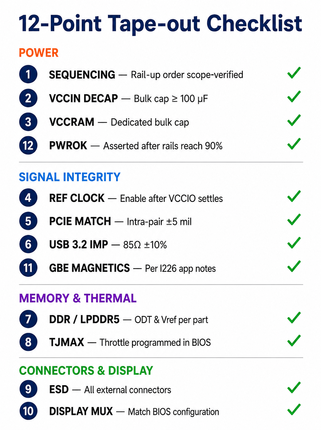
Read what matters: Vol 1 Power Management, Thermal, Supported Technologies, and Ball-out chapters cover ~90% of carrier-design work. Vol 2 covers signal integrity. Treat the rest as reference.
Use a public reference: The K1 carrier schematic (134×92mm) is one of the few public N100 reference designs. Read it alongside Vol 1 ball-out to sanity-check every signal.
Build the power tree right: convert 12V (or 5V) through the rail set defined in your N100 datasheet's Power Management Support chapter. Sequencing — auxiliary rails first, core rails next, PWROK last — is non-negotiable. Voltages and rail names come from your binding datasheet, not from third-party guides.
Mind the high-speed: 85 Ω differential impedance, intra-pair matching ±5 mil, ground stitching every 5 mm. Plane splits kill eye diagrams.
Run the 12-point checklist before tape-out: most "works on bench, fails in field" failures come from skipping three or more checklist items.
Companion to our Embedded Integration Guide. Last updated 2026-05-25 | Technical Documentation | Contact Sales


